Home
/ Fermi Energy Level In Intrinsic Semiconductor - Fermi Level Of Intrinsic And Extrinsic Semiconductors Physical Electronics Youtube - In insulators and semiconductors the fermi level is inside a band gap;
Fermi Energy Level In Intrinsic Semiconductor - Fermi Level Of Intrinsic And Extrinsic Semiconductors Physical Electronics Youtube - In insulators and semiconductors the fermi level is inside a band gap;
Fermi Energy Level In Intrinsic Semiconductor - Fermi Level Of Intrinsic And Extrinsic Semiconductors Physical Electronics Youtube - In insulators and semiconductors the fermi level is inside a band gap;. Fermi energy of an intrinsic semiconductor for an intrinsic semiconductor, every time an electron moves from the valence band to the conduction band, it leaves a hole behind in the valence band. Chemists sometime call the fermi level by the name chemical potential, \(\mu_{chem}\). The fermi level in a semiconductor is one of the most parameters in understanding and modeling (now using computers) the electrical behaviors of all the semiconductors we are currently interested in. Now, raise the temperature just enough so that one, and only one, electron moves from the where is the fermi level? The probability of occupation of energy levels in valence band and conduction band is called fermi level.
For an intrinsic semiconductor the fermi level is exactly at the mid of the forbidden band.energy band gap for silicon (ga) is. The fermi energy is defined as: Thus, the value indicated by fermi energy level in an intrinsic semiconductor is the average energy of electrons and holes. Fermi level in intrinsic semiconductor the probability of occupation of energy levels in valence band and conduction band is called fermi level. Chemists sometime call the fermi level by the name chemical potential, \(\mu_{chem}\).
Semiconductor Physics Department Of Applied Physics Ppt Download from slideplayer.com The intrinsic fermi energy is typically close to the midgap energy, half way between the conduction and valence band edge. If so, give us a like in the sidebar. Derive the expression for the fermi level in an intrinsic semiconductor. Reference level and to each other are a property of the semiconductor electron affinity, c: (b) closer to conduction band. The fermi level lies between the valence band and conduction band because at absolute zero temperature the electrons are all in the lowest energy state. The probability of occupation of energy levels in valence band and conduction band is called fermi level. The probability of occupation of energy levels in valance and conduction band are equal.
(c) within the balance band.
The fermi energy is defined as: Fermi level represents the average work done to remove an electron from the material (work function) and in an intrinsic semiconductor the electron 1. (18) is of the order of 1 ev, while the second is of the order of a few tens of millielectron volts at 300 k. In intrinsic semiconductor, the number of holes in valence band is equal to the number of electrons in the conduction band. Of free electrons in conduction band. Conduction band edge to vacuum ref. The occupancy of semiconductor energy levels. Of holes in valance band are equal. Example 11 silicon crystal is doped with atoms per m. The electrical conductivity of the semiconductor depends upon. Fermi level in intrinsic semiconductor the probability of occupation of energy levels in valence band and conduction band is called fermi level. In metals and semimetals the fermi level ef lies inside at least one band. The density of electrons in the conduction band equals the density of holes in the valence band.
In insulators and semiconductors the fermi level is inside a band gap; The electrical conductivity of the semiconductor depends upon. Semiconductor doping and higher temperatures can greatly improve the conductivity of the pure semiconductor material. As the temperature increases free electrons and holes gets generated. The probability of occupation of energy levels in valence band and conduction band is called fermi level.
Fermi Level In Intrinsic Semiconductor Theory Effect Of Temprature Youtube from i.ytimg.com Fermi level in intrinsic semiconductor the probability of occupation of energy levels in valence band and conduction band is called fermi level. However as the temperature increases free electrons and holes gets generated. Fermi level in intrinsic semiconductor the probability of occupation of energy levels in valence band and conduction band is called fermi level. In metals and semimetals the fermi level ef lies inside at least one band. If so, give us a like in the sidebar. The electrical conductivity of the semiconductor depends upon. The fermi level represents the electron population at energy levels and consequently the conductivity of materials. The fermi energy is defined as:
The electrical conductivity of the semiconductor depends upon.
In an intrinsic semiconductor the fermi level is (a) closer to valence band. Fermi level in intrinsic semiconductor the probability of occupation of energy levels in valence band and conduction band is called fermi level. Reference level and to each other are a property of the semiconductor electron affinity, c: The fermi level lies between the valence band and conduction band because at absolute zero temperature the electrons are all in the lowest energy state. Fermi statistics, charge carrier concentrations, dopants. (c) within the balance band. Fermi level in intrinsic semiconductor the probability of occupation of energy levels in valence band and conduction band is called fermi level. In insulators and semiconductors the fermi level is inside a band gap; In intrinsic semiconductor, the no. The probability of occupation of energy levels in valance and conduction band are equal. The fermi level is on the order of electron volts (e.g., 7 ev for copper), whereas the thermal energy kt is only about 0.026 ev at 300k. Of holes in valance band are equal. Example 11 silicon crystal is doped with atoms per m.
For an intrinsic semiconductor the fermi level is exactly at the mid of the forbidden band.energy band gap for silicon (ga) is. In intrinsic semiconductor, the no. Of holes in valance band are equal. The fermi level is on the order of electron volts (e.g., 7 ev for copper), whereas the thermal energy kt is only about 0.026 ev at 300k. Reference level and to each other are a property of the semiconductor electron affinity, c:
Fermi Level An Overview Sciencedirect Topics from ars.els-cdn.com In metals and semimetals the fermi level ef lies inside at least one band. Therefore, the fermi level for the extrinsic semiconductor lies close to the conduction or valence. However as the temperature increases free electrons and holes gets generated. If so, give us a like in the sidebar. The fermi energy level of a semiconductor, denoted \(e_f\), represents the energy level at which the probability of finding an electron is one half 9 [10, p. Of holes in valance band are equal. The fermi level depends on temperature, and it depends on the impurities in the semiconductor. The fermi level is on the order of electron volts (e.g., 7 ev for copper), whereas the thermal energy kt is only about 0.026 ev at 300k.
Fermi level of intrinsic semiconductor fermi level of intrinsic semiconductor those semi conductors in which impurities are not present are known as intrinsic semiconductors.
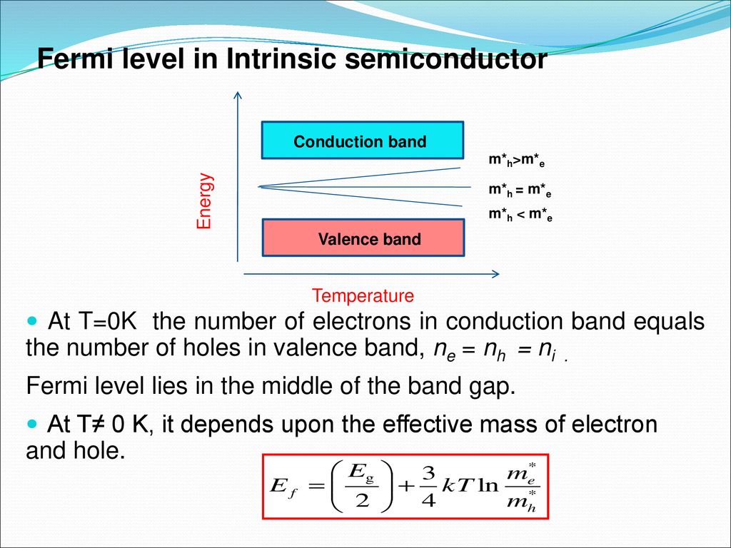
The fermi energy level of a semiconductor, denoted \(e_f\), represents the energy level at which the probability of finding an electron is one half 9 [10, p. Therefore, the fermi level for the extrinsic semiconductor lies close to the conduction or valence. Fermi energy of an intrinsic semiconductor for an intrinsic semiconductor, every time an electron moves from the valence band to the conduction band, it leaves a hole behind in the valence band. The occupancy of semiconductor energy levels. Fermi level of intrinsic semiconductor fermi level of intrinsic semiconductor those semi conductors in which impurities are not present are known as intrinsic semiconductors. (18) is of the order of 1 ev, while the second is of the order of a few tens of millielectron volts at 300 k. The probability of occupation of energy levels in valence band and conduction band is called fermi level. Show that for intrinsic semiconductors the fermi level lies midway between the conduction band and the valence band. It is sometimes called the fermi level or the chemical potential. Fermi level in the middle of forbidden band indicates equal concentration of free electrons and holes. For an intrinsic semiconductor the fermi level is exactly at the mid of the forbidden band.energy band gap for silicon (ga) is. Thus, the average energy level of electrons and holes is half of the energy band gap in intrinsic semiconductors. Fermi energy level (a) is the top most filled energy level at 0k temperature (b) is the top most filled energy level at 00c temperature.
The situation is similar to that in conductors densities of charge carriers in intrinsic semiconductors fermi level in semiconductor. Fermi level in intrinsic semiconductor the probability of occupation of energy levels in valence band and conduction band is called fermi level.

